Nearly invisible, never overlooked
Why go looking for the latest logistics trends and business insights when you can have them delivered right to you?
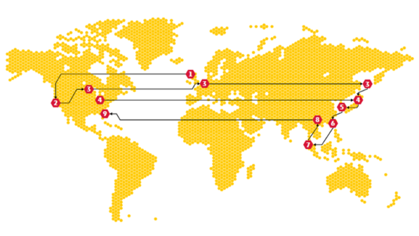
Global semiconductor value chain

- A UK firm licenses the IP on application process architecture
- A US-based fabless firm designs the chip
- Highly advanced manufacturing equipment is developed by companies in the US, Europe, or Japan
- Silicon dioxide is mined and refined in the US and sent to Japan to be melted down and grown into a giant single crystal called an ingot
- That ingot might then be sliced into wafers in South Korea
- The wafers may be shipped to fabs in Taiwan and turned into integrated circuits
- Individual chips are separated and packaged by an Assembly & Testing in Malaysia
- The chip is shipped to the smartphone OEM's assembly partner in China, to be incorporated into a circuit board inside the phone
- The smartphone is sold to a customer in the US.
Source: Strengthening the Global Semiconductor Supply Chain in an Uncertain Era (SIA and BCG)
Published: March 2023


